
The mission of Lagpat is to support a clean and green environment, we believe in giving back to the environment through working with the various charities including Orphanages and disability groups around the world! For the underprivileged families, we strive to support them by giving computers that are refurbished and can be reused.
Lagpat has been in Spain and Europe for over 20 years, the experience would enable us to innovate with the means to extract more reusable materials for further usage, and market the recycled items globally.
Global Services: focusing on logistics, the repair and distribution operations. Business solutions: in our services for the clients, confidentiality is kept and all recycling purpose. This procedure can be recorded via video and given to the clients for record purposes. Only a small fee for the video services will be charged. We have plans in the near future to bring in the best technology possible for stripping, extracting and process the e-waste. The logistic Services for collection are free.
The Logo of Lagpat is surrounded by three green arrows in a circular motion design, indicates a never ending process as a Recycling Service Provider. Our Strategy is to “Provide recycling Services and solutions to clients throughout Singapore and to divert materials from landfill to re-use, recycling and other forms of recovery”.
Lam Research designs and builds products for semiconductor manufacturing, including equipment for thin film deposition, plasma etch, photoresist strip, and wafer cleaning processes. Repeated throughout semiconductor manufacturing, these technologies help create transistors, interconnects, advanced memory, and packaging structures. They are also used for applications in related markets like microelectromechanical systems (MEMS) and light-emitting diodes (LEDs).
Lam's thin film deposition systems lay down the sub-microscopic layers of conducting (metal) or insulating (dielectric) materials that make up an integrated circuit. The processes require uniformity at the nanoscale level. The company employs electrochemical deposition (ECD) and chemical vapor deposition (CVD) technologies to form copper and other metal films for conducting structures. Atomic layer deposition (ALD) is also used for tungsten metal films in features like contacts and plugs, which are vertical connections between metal lines in multilevel interconnect chip designs.
Plasma-enhanced (PE) CVD and ALD technologies create dielectric films for a wide range of insulating parts. For gapfill processes, which require depositing dielectric material into narrow spaces, Lam uses high-density plasma (HDP) CVD technology. PECVD and ALD are also used to form hardmasks, layers which can be removed to improve circuit patterning processes.
Lam Research uses proprietary technology in its equipment for plasma etch, the process of selectively removing materials from the surface of a wafer in order to create the semiconductor device's features and patterns. The equipment helps chip manufacturers carve small features such as those needed for the latest multiple patterning sequences, transistors, and advanced memory structures, which involve increasingly complex film stacks and ever higher aspect ratio structures. The company uses reactive ion etch (RIE) and atomic layer etching (ALE) to shape a variety of conductive and dielectric features. The company's deep RIE technologies help create structures for applications like MEMS and through-silicon vias (TSVs).
Lam's dry strip systems use plasma technology to selectively remove the photoresist mask following a range of front-end wafer processing and advanced packaging applications.
Lam Research's wet spin clean and plasma-based bevel clean products remove particles, residues, and films from the wafer surface before or after adjacent processes. The company's spin wet clean technology is used between chip-processing steps to remove yield-limiting residues and defects. Lam's bevel clean technology directs a plasma at the very edge of the wafer to clean unwanted particles, residues, and films. If not removed, these materials can impact yield if they flake off and re-deposit on the device area during subsequent manufacturing steps.

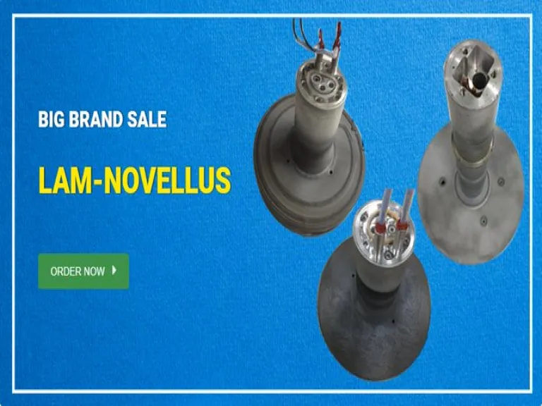
We are specialized in selling Lam Novellus Products. The items are either NEW sealed boxed, NEW open box, USED, TESTED and good condition. Please make your best offer!!! Looking for the low cost Lam Novellus in USA? Lagpat offers the high quality and low cost Lam Novellus. Shop our cart now! Find the best deals for low cost Lam Novellus products in USA at Lagpat. Shop online here. Get the best deals on Lagpat for Lam Novellus products in USA. Shop with confidence. To get more details about the Lam products in UK? Please click here!


- Rescue Service said. The spokesman told The Associated Press that rescuers were looking for more survivors in the ocean.
.png)
- It almost probably has a robe, if your home has a fireplace. You are fortunate! You are fortunate! A cloak is a reason to celebrate

- There is no steering apparent of the truth that inside of our present day modern society we assume our children for currently being at school

- The overcrowded school rooms, schoolyard violence, and obtain to illegal drug that has been creating inroads during the Ga